Metallization of self-assembled particle layers for transparent conductor applications
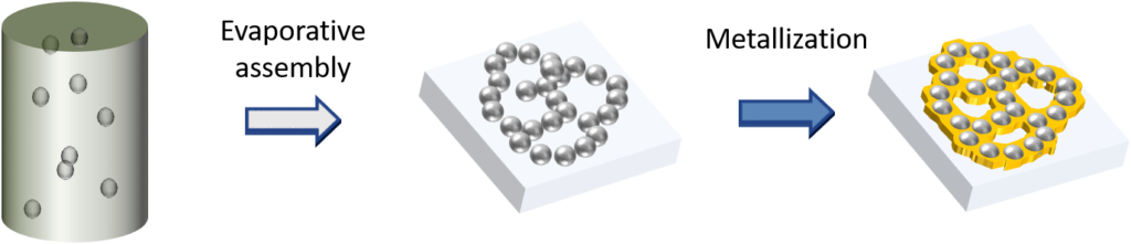
There is a significantly growing demand for transparent conductive coatings for use in modern optoelectronics applications such as personal electronics, displays, photovoltaics and adaptive windows. In particular, incumbent technologies such as indium tin oxide (ITO) which have long dominated the rigid substrate market are expected to meet fundamental challenges in the form of raw materials costs (Indium) and applicability to flexible substrates. Various solutions currently under investigation include silver nanowires, carbon nanotubes, graphene, conducting polymers etc. Since these all have their shortcomings, there is a great need for the investigation of alternative, preferably more versatile, approaches for the structuring of metal-containing films. To experimentally and theoretically explore the use of particle-layer templated transparent conducting films a strategic alliance linking four university groups with an industrial partner (BASF SE) was established by the Cluster of Excellence EAM. Robin Klupp Taylor was coordinator of this project and supervisor of one of the sub-projects. In this we successfully realized the untested idea from that capillary “bridges” between colloidal silica particles in a close packed monolayer could be used as the basis to form a long-range (~cm) conductive network.
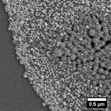
An impressive range of possibilities for hierarchical 2D silica particle network film deposition were developed using both model colloidal particles and commercial silica.
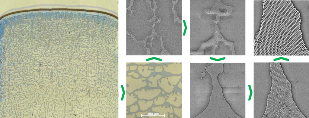
Simple metallization techniques were also established, the preference being for a two-step procedure whereby the template film is first treated with a reactive silver ink to form silver seeds in the interstices between the template particles followed by copper plating in a standard electroless plating bath. Regarding film performance transmissions of up to 75%, haze factors below 3.5% and sheet resistances below 285 Ω/□ could be achieved.